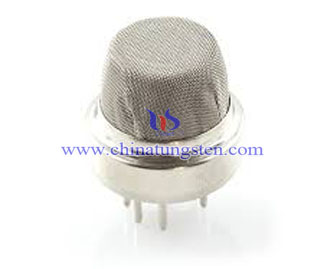
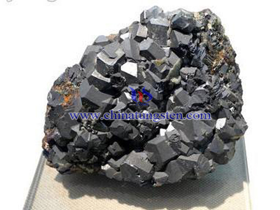
Meso Porous Silicon WO3 Gas Sensor
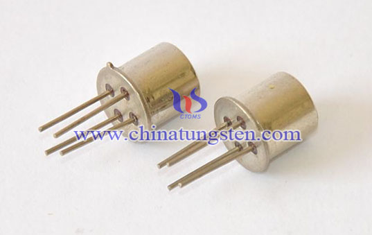
Porous silicon was found in 1956 by scientists in Bell Labs, when they were studying the anodic oxidation corrosion polishing process. The formation mechanism of porous silicon charge exchange is conducted between the surface of silicon semiconductor and the HF solution. According to different aperture sizes and porosity can be divided into three types, namely large holes silicon (Macro-PS), mesoporous silica (Meso-PS) and nanoporous silicon (Nano-PS).
Principle of gas sensors based on porous silicon different gases change the physical characteristics of the PS-based. Porous silicon surface adsorbs gas molecules change of free carrier concentration, or due to changes caused by concentrated gas wells dielectric constant, causing changes in conductance or capacitance.
Below are the producing method of meso porous tungsten oxide gas sensor:
Deposition of tungsten oxide1.Coating Process: Fix prepared meso porous silicon substrate on the sample holder, and then start using the DPS-Ⅲ type ultra-high vacuum magnetron sputtering coating machine for thin film coating system.
2.Sputtering tungsten oxide thin film
3.Deposition of Pd electrode
Although meso porous silicon WO3 gas sensor has a lower operating temperature, it can not have high sensitivity and low response / recovery time at the same time. It is related to micro size of meso porous silicon and tungsten oxide. Mesoporous silica pore size in 30nm or less, and WO3 particle size after annealing at about 70 nm, which led to the crystalline WO3 particles after the meso porous silica pores blocked. When WO3 layer is thin, the particles after heat treatment began covering the mesoporous silicon surface, but not to fill the voids. This structure on the one hand, is not conducive to the spread of gas, but also reduces the specific surface area of the gas sensor.

